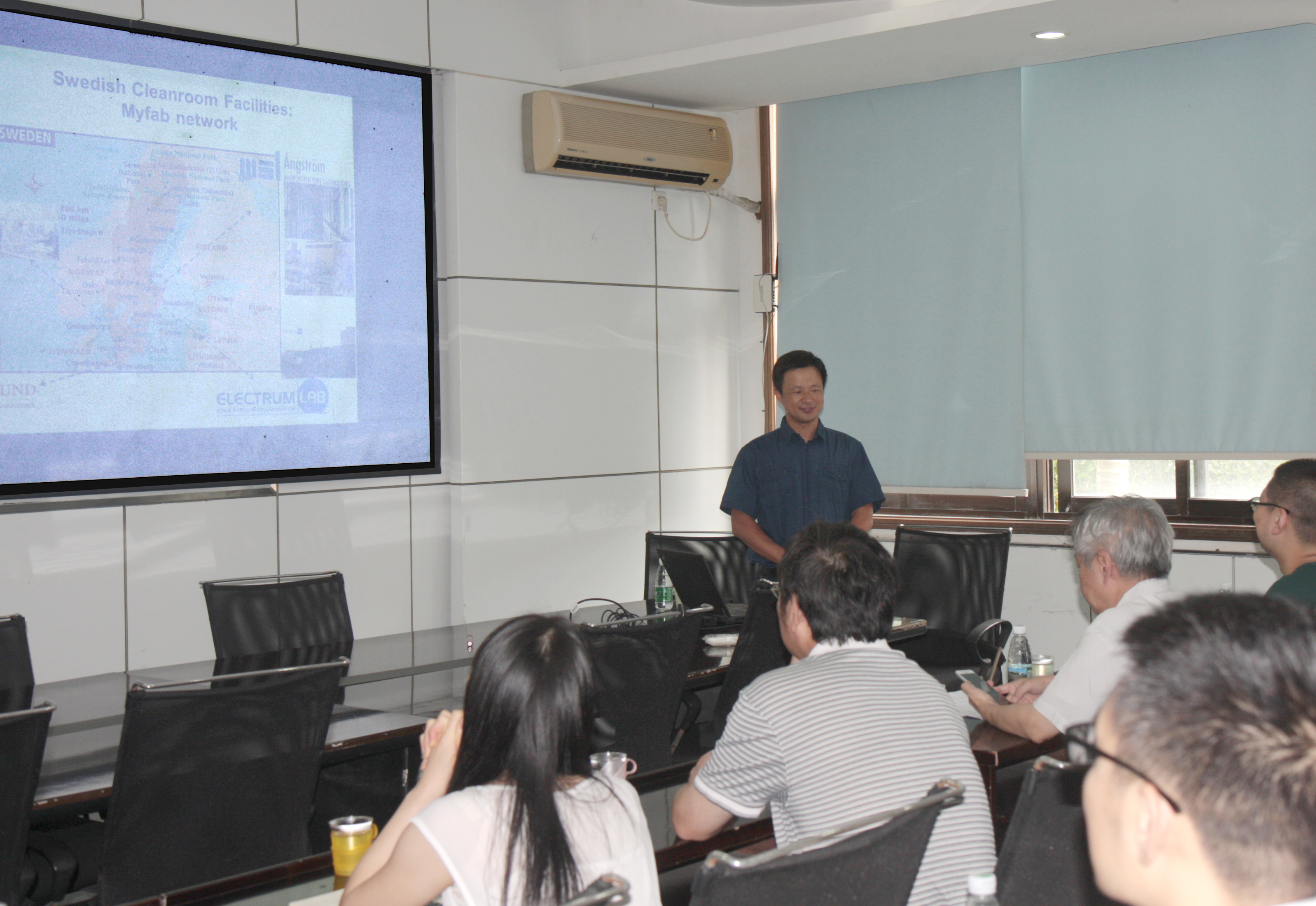
报告题目:Processing graphene: the key to the success in electronic application
报告人: 张志滨副教授,瑞典乌普萨拉大学工程科学系固态电子研究部
时间: 10月8日(周六) 上午10:00
地点: 化学楼二楼会议室-234
报告摘要:
With the progressive advancement of graphene research, the discovered various unique and exceptional properties in electronic and electrical, thermal, mechanical and optical aspects have excited enormous people’s imagination for graphene’s applications. A success to make use of the exceptional properties and achieve real killing applications of graphene requires overcoming the challenges encountered during the processing of graphene. In this talk, I give a brief overview on our effort of technique development of CVD-grown graphene (CVD-G) and pristine graphene nanoplatelets (p-GNPs). A modified process that provides high quality transfer of CVD-G is presented that is verified by means of surface enhanced Raman scattering effect with Au nanoparticles. A two-in-one process for device fabrication with photolithography and atomic-layer deposition (ALD) technology is developed that leads to a good control over the interface in graphene field-effect transistors (GFETs). Thin-film deposition by means of sputtering on a CVD-G is evaluated and the associated defect creation in the CVD-G is characterized. As for GNPs, the potential of the application in printed electronics is high. The use of GNPs offers a route to achieve reliable low-resistivity interconnections on polymeric substrates prepared at low temperature. Printed GNPs thin films in general suffer from low performance due to limited carrier density and numerous inter-flake junction resistances, poor thermal stability in doping, and low efficiency in material production as compared to flakes with reduced graphene oxide. We have developed procedures based on liquid-phase shear mixing and electrochemical exfoliation process for scalable production of few-layer p-GNPs and ink formulation for ink-jet printing process. Printed GNP films are enhanced in electrical conductivity and figure of merit of transparent conductive films by means of low temperature halogen doping procedure which exhibits excellent thermal stability.
参考文献:
1. Patrik Ahlberg, Malkolm Hinnemo, Man Song, Shi-Li Zhang and Zhi-Bin Zhang*, “A two-in-one process for reliable graphene transistors processed with photo-lithography”, Applied Physics Letters, 107, 203104, 2015.
2. Malkolm Hinnemo, Patrik Ahlberg, Carl Hägglund, Wencai Ren, Hui-Ming Cheng, Shi-Li Zhang, Zhi-Bin Zhang*, “Scalable residue-free graphene for surface-enhanced Raman scattering” Carbon, 98, 567, 2016.
3. P. Ahlberg, T. Nyberg, Shi-Li Zhang and Zhi-Bin Zhang*, “Toward synthesis of oxide films on graphene with sputtering based processes”, Journal of Vacuum Science & Technology B 34, 040605 (2016).
4. Subimal Majee, M.Song, S.–L. Zhang, Z.-B. Zhang*, Scalable inkjet printing of shear-exfoliated graphene transparent conductive films. Carbon, 102, 51, 2016.
5. Subimal Majee, Jie Zhao, Man Song, C. Liu, Biao Wu, S.-L Zhang and Z.-B Zhang, Ink-jet printed highly conductive and reliable pristine graphene patterns achieved with water-based ink and aqueous doping processing, submitted.

个人简历:

|
2001年中科院上海应用物理研究所博士毕业,2001年到2002年比利时鲁汶大学做访问学者,2002年到2004年瑞典皇家工学院信息与通讯学院做博士后,之后留校任终身研究员。2009年作为核心管理和技术骨干参与由皇家工学院,瑞典工业创新署,和数家瑞典造纸业巨头联合成立的创新中心(iPack)并组建并负责印刷器件课题组。2011年到乌普萨拉大学技术学院工程科学系固态电子实验室组建柔性电子课题组。2009年到2013年复旦大学微电子学院高级访问学者。2015年起任陕西省西北大学化学材料学院兼职教授。张志滨的研究领域涉及碳纳米管,石墨烯,和复合纳米电子材料及其在印刷电子,柔性电子,薄膜晶体管和电路,传感器,电致变色器件,射频电子等方面的应用研究,同时也涉及柔性热电器件和面向热电应用的硅基薄膜材料的研究。目前在著名专业杂志以发表论文60余篇,其中以第一作者和通讯作者30余篇。 |
课题组网页:http://www.teknik.uu.se/fasta-tillstandets-elektronik/forskningsomraden/flexibel-elektronik/