Title: Processing graphene: the key to the success in electronic application
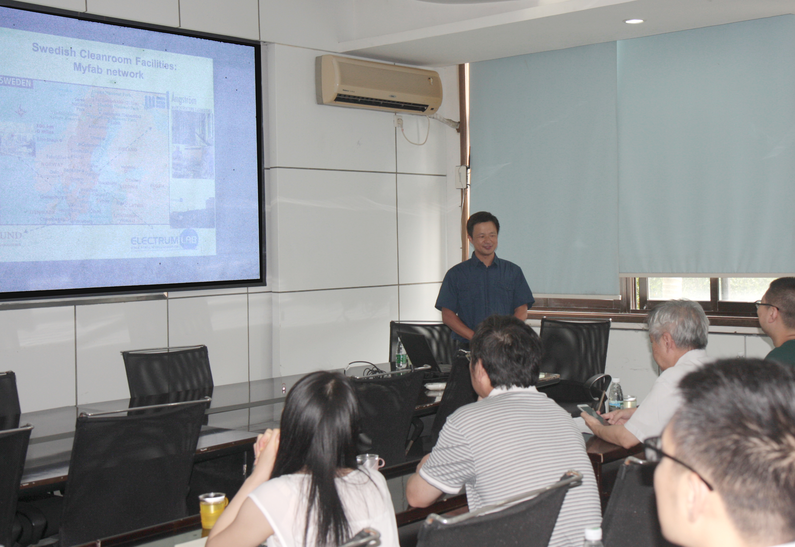
Speaker: Assoc. Prof. Zhi-Bin Zhang, Uppsala University, Sweden
Date/Time: 10:00 AM, Oct.8, 2016 (Sat.)
Location: Room 234 in the Chemistry Building
Abstract: With the progressive advancement of graphene research, the discovered various unique and exceptional properties in electronic and electrical, thermal, mechanical and optical aspects have excited enormous people’s imagination for graphene’s applications. A success to make use of the exceptional properties and achieve real killing applications of graphene requires overcoming the challenges encountered during the processing of graphene. In this talk, I give a brief overview on our effort of technique development of CVD-grown graphene (CVD-G) and pristine graphene nanoplatelets (p-GNPs). A modified process that provides high quality transfer of CVD-G is presented that is verified by means of surface enhanced Raman scattering effect with Au nanoparticles. A two-in-one process for device fabrication with photolithography and atomic-layer deposition (ALD) technology is developed that leads to a good control over the interface in graphene field-effect transistors (GFETs). Thin-film deposition by means of sputtering on a CVD-G is evaluated and the associated defect creation in the CVD-G is characterized. As for GNPs, the potential of the application in printed electronics is high. The use of GNPs offers a route to achieve reliable low-resistivity interconnections on polymeric substrates prepared at low temperature. Printed GNPs thin films in general suffer from low performance due to limited carrier density and numerous inter-flake junction resistances, poor thermal stability in doping, and low efficiency in material production as compared to flakes with reduced graphene oxide. We have developed procedures based on liquid-phase shear mixing and electrochemical exfoliation process for scalable production of few-layer p-GNPs and ink formulation for ink-jet printing process. Printed GNP films are enhanced in electrical conductivity and figure of merit of transparent conductive films by means of low temperature halogen doping procedure which exhibits excellent thermal stability.
References:
1. Patrik Ahlberg, Malkolm Hinnemo, Man Song, Shi-Li Zhang and Zhi-Bin Zhang*, “A two-in-one process for reliable graphene transistors processed with photo-lithography”, Applied Physics Letters, 107, 203104, 2015.
2. Malkolm Hinnemo, Patrik Ahlberg, Carl Hägglund, Wencai Ren, Hui-Ming Cheng, Shi-Li Zhang, Zhi-Bin Zhang*, “Scalable residue-free graphene for surface-enhanced Raman scattering” Carbon, 98, 567, 2016.
3. P. Ahlberg, T. Nyberg, Shi-Li Zhang and Zhi-Bin Zhang*, “Toward synthesis of oxide films on graphene with sputtering based processes”, Journal of Vacuum Science & Technology B 34, 040605 (2016).
4. Subimal Majee, M.Song, S.–L. Zhang, Z.-B. Zhang*, Scalable inkjet printing of shear-exfoliated graphene transparent conductive films. Carbon, 102, 51, 2016.
5. Subimal Majee, Jie Zhao, Man Song, C. Liu, Biao Wu, S.-L Zhang and Z.-B Zhang, Ink-jet printed highly conductive and reliable pristine graphene patterns achieved with water-based ink and aqueous doping processing, submitted.

|
Biography:

|
Dr. Zhi-Bin Zhang is associate professor (docent) in electronics and group leader of flexible electronics research group in Department of Engineering Sciences at Uppsala University, Sweden. He received his PhD degree in Shanghai Institute of Applied Physics, Chinese Academy of Sciences in 2001. He worked as a postdoctor from 2002 for two years and then as researcher for eight years in the school of information and com munication technology at Royal Institute of Technology (KTH) before moved to Uppsala University in 2011. During working in KTH, he had joined the Swedish 10-year academy-industrial joint research center for intelligent packaging (iPack center) as leader of “printed devices” group with 2 academic research groups and 5 industrial R&D sessions. In Uppsala University, he works as PI in a project funded by Swedish Research Council on developing thermoelectric devices using silicon and Co-PI in a frame-work project funded by Swedish Strategic Research Foundation on Carbon based high speed electronic systems. He has published over 60 peer-review journal articles with h-index 14 (google scholar) around 10 conference contribution and given around 20 invited talks. His research spans from technology of carbon nanotubes, graphene and composites for device application, printed electronics, deformable electronics and thermoelectrics for energy harvesting. |
Group page: http://www.teknik.uu.se/fasta-tillstandets-elektronik/forskningsomraden/flexibel-elektronik/